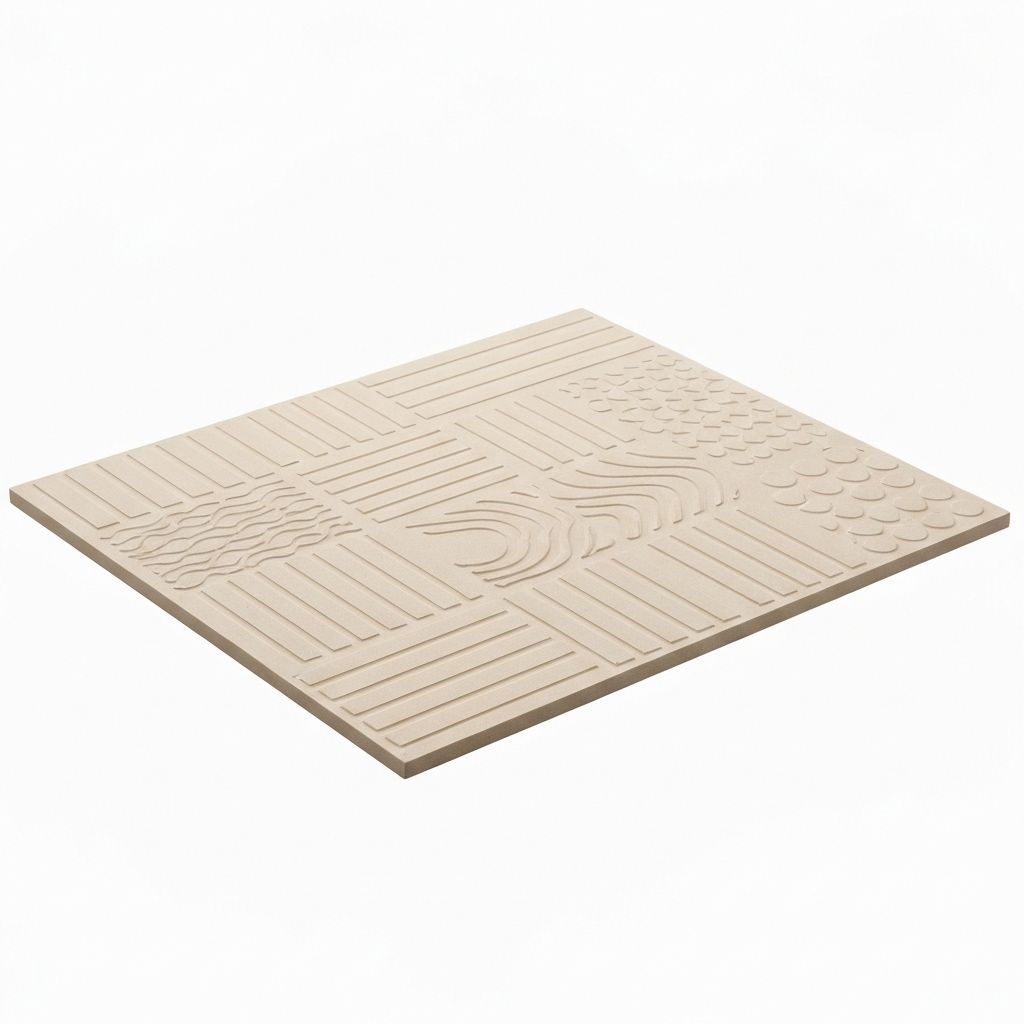
Screen Printing
High-resolution thick film pattern application for electronic and functional ceramics
Precision Thick Film Deposition
Our precision screen printing services apply thick film patterns, coatings, and functional layers to ceramic substrates with exceptional accuracy and repeatability. We specialize in fine-line printing for electronic circuits, sensors, and decorative applications.
With both automated and manual printing capabilities, we handle everything from rapid prototyping to high-volume production, ensuring consistent quality and excellent layer-to-layer registration.
Screen Printing Capabilities
Fine Line Printing
- Line widths down to 100μm
- High-resolution pattern definition
- Tight dimensional tolerances
- Excellent edge definition
Multi-Layer Processing
- Precision layer-to-layer registration (±25μm)
- Multiple conductor and dielectric layers
- Crossover and via structures
- Complex circuit architectures
Production Flexibility
- Automated and manual printing options
- Various substrate sizes and materials
- In-line drying and firing capabilities
- Rapid prototyping to production volumes
Applications
Hybrid Circuits
Conductive traces and resistor networks
Sensors
Thick film sensing elements and electrodes
Heaters
Resistive heating patterns
LED Substrates
Metallization for LED arrays
RF Components
Antennas and microwave circuits
Solar Cells
Front and back contact metallization
Automotive Electronics
Sensor circuits and control modules
Medical Devices
Biosensor electrodes and circuits
Decorative Ceramics
Functional and aesthetic patterns
Why Choose Our Screen Printing Services
High Resolution
Fine line capability and excellent pattern definition for complex designs
Excellent Registration
Precise layer-to-layer alignment for multi-layer structures
Cost-Effective
Economical solution for medium to high volume production
Rapid Turnaround
Quick setup and processing for prototypes and short runs
Material Versatility
Compatible with various inks and substrate materials
Quality Assurance
In-process inspection and documentation for consistent results
Ready to Start Screen Printing?
Contact our screen printing team to discuss your thick film application needs